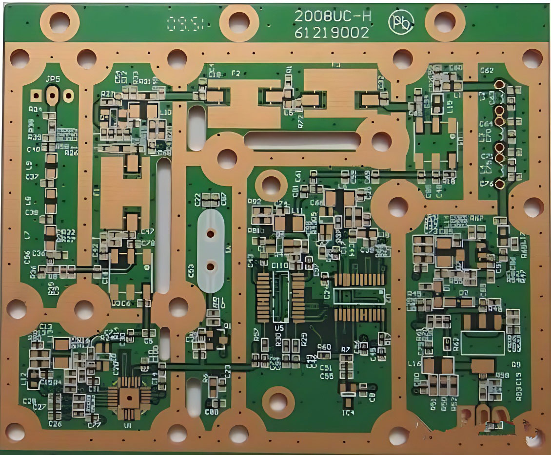
In PCB (Printed Circuit Board) manufacturing, surface finish treatment serves as a crucial step to safeguard copper conductors, enhance soldering performance, improve electrical properties, and prolong the lifespan of PCBs. Among the prevalent surface finish techniques, immersion gold (ENIG, Electroless Nickel/Immersion Gold), electrolytic gold plating, and hot air solder leveling (HASL) each possess unique attributes tailored for diverse application scenarios.
1. Immersion Gold (ENIG)
► Characteristics:
- Process: Immersion gold employs a chemical electroplating method where a layer of nickel is deposited onto the copper surface, followed by a thin layer of gold over the nickel to prevent nickel oxidation.
- Layer Thickness: The gold layer in immersion gold is typically thin, ranging from 0.025 to 0.1 micrometers, yet it offers exceptional electrical connectivity.
► Advantages:
- Excellent Flatness: The immersion gold surface is remarkably flat, ideal for BGA (Ball Grid Array) packages with fine-pitch and high-density wiring.
- Superior Solderability: The immersion gold layer exhibits inhibited oxidation, providing stable performance during soldering and effectively reducing the incidence of cold solders and false soldering.
- High Reliability: The immersion gold layer boasts strong stability, corrosion resistance, and wear resistance, making it suitable for circuits demanding high reliability.
► Disadvantages:
- Relatively High Cost: The immersion gold process is relatively costly and unsuitable for cost-sensitive projects.
- Complex Process: The immersion gold process involves multiple layers of electroplating with stringent process requirements, making it apt for precision circuits.
► Applications:
High-density, high-precision PCBs such as mobile phone motherboards, computer motherboards, and high-end communication equipment.
Applications requiring high soldering reliability, like high-density designs with BGA packages.
2. Electrolytic Gold Plating
► Characteristics:
- Process: Electrolytic gold plating is an electroplating technique where a layer of nickel and a layer of gold are electroplated onto the copper surface, commonly used for edge connectors or areas requiring high abrasion resistance.
- Layer Thickness: The electrolytic gold layer is thicker, typically ranging from 0.5 to 3 micrometers, offering good fatigue resistance.
► Advantages:
- High Abrasion Resistance: The thicker gold layer, combined with its hardness, suits connectors, and edge connectors subject to intermittent mating and unmating, providing superior wear resistance.
- Low Contact Resistance: The gold layer exhibits excellent conductivity and low contact resistance, suitable for circuits requiring stable electrical conduction.
- Low Surface Oxidation: The electrolytic gold surface is resistant to oxidation, maintaining good soldering and conductivity over time.
► Disadvantages:
- Increased Cost: The thicker gold layer increases material costs.
- Poor Solderability: Thicker gold layers can lead to soldering issues, thus primarily used for edge connectors and high-contact requirement areas.
► Applications:
- Edge connectors, gold fingers, and high-frequency mating contact areas.
- High-precision, high-reliability circuits requiring abrasion resistance, such as servers, communication devices, and luxury custom systems.
3. Hot Air Solder Leveling (HASL)
► Characteristics:
- Process: HASL utilizes a hot air solder leveling process where a layer of tin-lead alloy is applied to the copper surface and then smoothed by hot air blowing after high-temperature heating, resulting in a smooth soldering layer.
- Surface Irregularity: The HASL surface may exhibit irregularities upon cooling, unsuitable for high-density, fine-pitch designs.
► Advantages:
- Low Cost: The HASL process is straightforward and cost-effective, suitable for mass production.
- Excellent Solderability: The tin layer offers good soldering and wettability, suitable for both manual and automated soldering.
- Ease of Repair: The tin layer performs well during rework and desoldering without damaging the pads.
► Disadvantages:
- Unsuitable for High-Density Designs: The HASL surface's irregularities make it unsuitable for fine-pitch components like BGAs, prone to bridging issues.
- Oxidation Susceptibility: HASL boards are prone to oxidation, and deteriorating soldering performance over time, suitable for products requiring rapid production and deployment.
► Applications:
Consumer electronics such as appliances, toys, and low-end communication devices.
Applications like traditional electronic control boards require good solderability but not high precision.
| Approach | Advantages | Disadvantages | Applications |
|---|---|---|---|
| * Immersion Gold (ENIG) | Excellent flatness, high welding reliability, and good corrosion resistance. | High cost and complex manufacturing process. | High density for precise PCB positioning, such as in smartphone and computer motherboards. |
| * Electrolytic Gold Plating | High wear resistance, low contact resistance, and oxidation resistance. | High cost and poor weldability. | Edge connectors, and gold fingers, for devices requiring intermittent mating and unmating. |
| * Hot Air Solder Leveling (HASL) | Low cost, good weldability, and suitable for mass production. | Uneven surface and prone to oxidation. | General consumer electronics with low precision requirements. |
Choosing the appropriate surface finish for PCBs necessitates a holistic consideration of cost, durability, soldering performance, and equipment requirements to ensure that the PCB's performance and reliability meet design specifications. Each surface finish offers unique benefits tailored to specific applications, making it essential to select the most suitable option based on the project's demands.


